TOP SILICON WAFERS SOLUTION IN APAC 2025
2004年に2000万円の資金を前職の会社から出資していただき米国で設立したMicro Semiconductor Researches, LLC.(以降MSRという)。その後2006年に出資金全額を前職の会社に支払い完全独立した。2012年には東京に現地法人である株式会社マイクロセミコンダクターリサーチを設立。2004年から数え20年が経った。従業員はなく東京にアシスタントが一人いるだけだ。
仕事は半導体の製造サービス。カリフォルニアのシリコンバレーの他オレゴン州、ワシントン州、ドイツ、スウェーデンにある半導体製造工場の協力を得て顧客の要望にあった半導体を作るサービスだ。また半導体基板であるシリコンウェーハの供給もアメリカやマレーシアにある工場の協力で行っている。
特定の顧客があるわけではない。ホームページからの問い合わせによりMSRへ仕事の話が舞い込んでくる。一つひとつの案件は小さいものばかりだ。しかも簡単なプロセスではないものが多い。顧客の要望をじっくりと聞いて、まずは断ることはしない。なんとかできないものなのか、必ず考える。前述した工場はそれぞれ特徴があり、このプロセスならこの工場へ、と感を働かせ工場へ問い合わせする。一工場だけでは完結しないプロセスもあり、その場合は複数工場への掛け持ちプロセスを行う。
数量はいつも最小ロットである。厄介なプロセスの割には小ロットなので利益は多くない。リピート注文でもあればまだいいのだが、ほとんどない。
顧客は研究所や開発担当が多く、半導体製造装置メーカーや薬品メーカーなど半導体サプライチェーンからの依頼ばかりだ。それでも次世代半導体開発を担っているんだ、という気概で仕事をしている。
ある顧客との打ち合わせの時に聞いたのだが、「グループ会社でもこの製品を製造しているので問い合わせたのだが断られ、その他にもいろいろなところに問い合わせしたけどみんな断られ、最後に部下に御社へ聞いてみたら、ということで問い合わせたら快く仕事を受けてくれてサンプル発注したら良好な結果が出たので採用することにした。」という経緯もあった。
失敗もたくさんある。散々打ち合わせして見積もりまで提出し、発注する段階になりできません、ということがあり、顧客からはこっぴどく怒られたこともある。
そんなことを繰り返しながらいままで20年間半導体の製造サービスを生業としてきた。
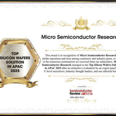
今年の4月に米半導体専門誌Semiconductor Review APACから問い合わせがありTOP SILICON WAFERS SOLUTION IN APAN 2025に選定したいのでインタビューをしたい、との申し出があった。どこで聞きつけたのか知る由もないのだが、いわれるままにインタビューを受けた。
どうも半導体開発用に小ロットでプロセスサービスしているのが評価されたようだった。そしてその専門誌の記事にも掲載された。記事の内容は以下の通り。
Micro Semiconductor Research
Wafers for the Next Wave of Innovation
As semiconductor technologies advance and R&D cycles accelerate, there is a growing need for
high-quality, small-volume test wafers that support rapid process development and materials
validation. For semiconductor equipment manufacturers and materials suppliers offering high-
purity gases and specialty chemicals, these wafers provide a cost-effective way to simulate real
manufacturing conditions without committing to large-scale fabrication runs.
However, sourcing these test wafers for early-stage research is a persistent challenge.
Traditional wafer suppliers are built for high-volume production, not the flexibility and
responsiveness that early-stage research demands.
Micro Semiconductor Research (MSR) was founded to close that gap. Specializing in low-
volume, high-complexity wafer solutions, MSR plays a vital role for R&D teams in
semiconductor equipment and materials companies. These innovators rely on high-quality
wafers to simulate real production environments, whether calibrating etch and deposition tools
or testing the purity of specialty gases and chemicals.
Offering customized wafer processing, including refurbished prime silicon and advanced
bonding capabilities, MSR enables rapid iteration, precise validation, and true development
freedom. Where others require high minimums and rigid specs, MSR delivers flexibility, speed,
and deep technical insight.
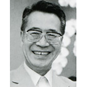
“We work closely with customers who are developing next-generation technologies, and our
goal is to provide exactly what they need so they can keep moving forward without
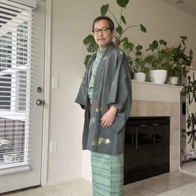
compromise,” says Seiji Yamashita, president.
What sets MSR apart is its ability to take on low-volume, high-specification orders that fall
outside the interest of conventional fabs. While larger players typically require high minimums,
MSR regularly fulfills orders as small as 10 or 50 wafers.
Several major Japanese companies have turned to MSR with wafer requirements that others
deemed too difficult or too small to fulfill. MSR not only accepted the challenge—it delivered,
helping bring ambitious prototypes one step closer to reality. The willingness to accommodate
small batches and a deep understanding of semiconductor processes makes MSR a critical
enabler for innovation-driven companies and R&D teams iterating at the edge of feasibility.Many of MSR’s clients include universities, research labs and advanced semiconductor firms
that turn to the company with projects involving unusual substrates or specialized needs like
SOI wafers, where standard suppliers either decline the work or lack the capability.
One major Japanese company, for example, spent months searching for a vendor to fulfill a
technically complex wafer request. No one would take it on until they approached MSR. The
company produced a test batch that met strict evaluation criteria, leading to an ongoing
partnership.
MSR also identifies opportunities in areas others overlook. The company sources high-quality
silicon wafers that were originally scrapped due to non-crystalline issues. These wafers are
procured at low cost in the U.S. and then refurbished to prime condition in Japan. Once
restored to prime condition, these wafers are supplied with full Certificates of Conformance,
offering customers a more affordable alternative to newly manufactured prime wafers. This
capability is cost-effective as well as represents a key growth area for the company moving
forward.
Beyond silicon, MSR is expanding its expertise in wafer bonding with next-generation materials
such as silicon carbide (SiC) and piezoelectric oxides (PO). Developing techniques to bond these
with traditional silicon substrates, the company is carving out a position at the leading edge of
advanced semiconductor integration, a space where customization, agility and innovation
intersect.
As semiconductor technologies advance and novel materials redefine performance limits, MSR
stays at the forefront, delivering tailored wafer solutions that power the next generation of
innovation.